
Solutions
fastMES for Semiconductor
fastMES for Semiconductor is an MES specialized for semiconductor companies that process wafers and package chips. It controls both front-end and back-end FAB processes and manages recipes and characteristics down to the individual wafer.
Benefit
Real-time collection and analysis of process data / Precise root-cause tracing of abnormal yield / Automatic generation of customer-specific tags and test reports / Real-time quality tracking by customer / Automatic quality judgment of measurement data / Process standardization / Lower compliance costs
Conceptual Diagram
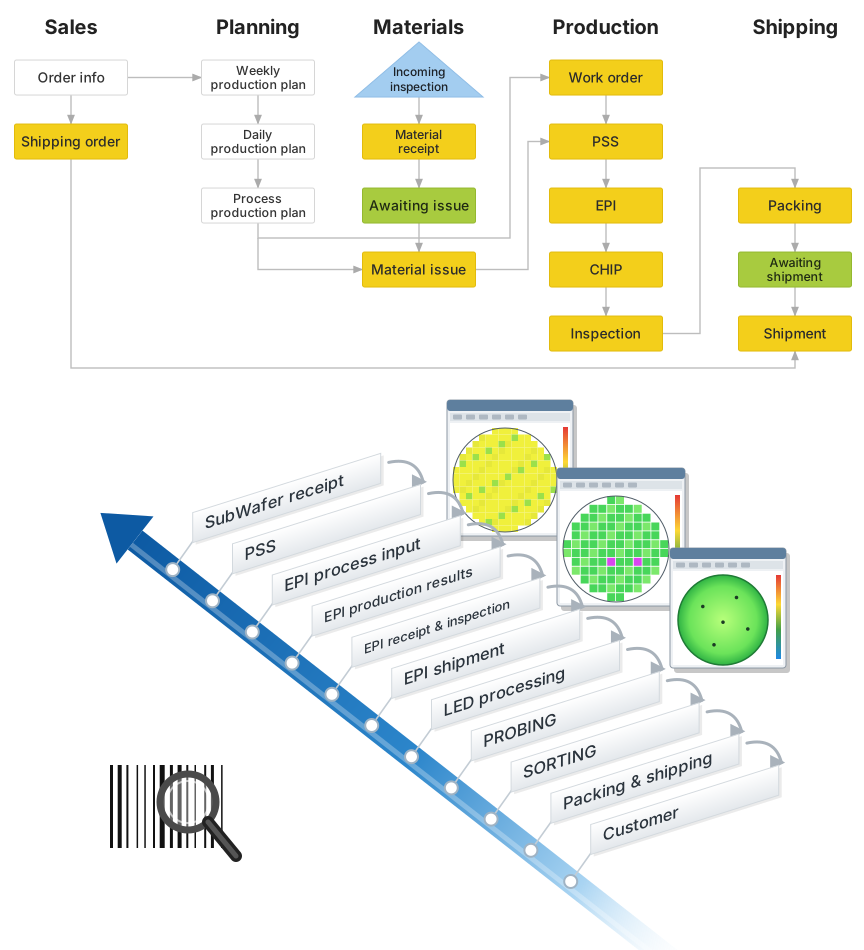
MES sits at the center of the system and serves as the information hub of the entire manufacturing system. It receives basic information such as production and delivery plans and product and material data from the ERP system and carries out the actual production activities. It manages the entire flow of semiconductor manufacturing (wafer fabrication and packaging for memory, non-memory, foundry, LED and more) and replaces conventional traveler sheets and run sheets.

Hardware Configuration Diagram
Key features: integration with ERP systems such as SAP and Oracle, real-time process status monitoring, real-time trends of key process parameters, data integration using barcodes and RFID, and real-time LOT tracking (LOT Traceability System) covering material receipt, production and shipment

Process
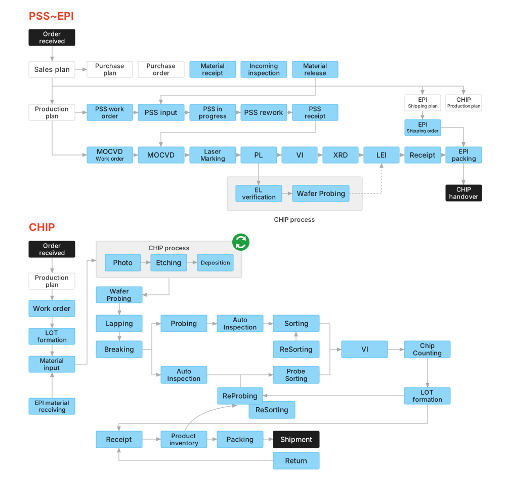
Semiconductor: Detailed Chip Process
Key process data from wafer receipt through front-end processes, probe testing, back-end processes and packaging is managed not only per wafer but down to the chip, the smallest unit, enabling forward and backward tracing from chip level to wafer and carrier lot.
Software Configuration Diagram
fastMES for Semiconductor provides processes tailored to semiconductor manufacturing, with integrated management of lot splitting and merging, routes, recipes and parameter settings, as well as real-time LOT tracking.

Main Screen

MES MAIN

Tracking by carrier, wafer and chip

Real-Time Quality Analysis

Measurement result analysis

Chip yield analysis

Real-time equipment status
Benefits
- 2~100%
Better production data
collection - 10~100%
Less
paperwork - 5~82%
Shorter
production cycle - 2~63%
Higher
quality - 3~60%
Shorter production
lead time - 3~50%
Less
WIP inventory
Higher yield and quality
- Real-time process capability analysis
- Real-time tracking of defect and quality data
- Strict preservation of manufacturing records
- Precise root-cause tracing of abnormal yield
Customer satisfaction
- Meets diverse customer requirements
- Real-time quality tracking by customer
- Customer priorities set according to production plans
- Automatic generation of customer tags and test reports
Lower data collection and analysis costs
- Process standardization
- Storage of all production records
- Automatic quality judgment of measurement data
- Real-time quality analysis and tracking
- Lower compliance costs